 2024/5/29 16:31:40
 168
168
·2-V to 5.5-V VCC Operation
·Max tpd of 8.5 ns at 5 V
·Typical VOLP (Output Ground Bounce)<0.8 V at VCC = 3.3 V, TA = 25°C
·Typical VOHV (Output VOH Undershoot)>2.3 V at VCC = 3.3 V, TA = 25°C
·Support Mixed-Mode Voltage Operation on All Ports
·Latch-Up Performance Exceeds 250 mA Per JESD 17
·ESD Protection Exceeds JESD 22
− 2000-V Human-Body Model (A114-A)
− 200-V Machine Model (A115-A)
− 1000-V Charged-Device Model (C101)
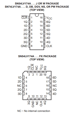
description/ordering information
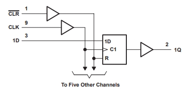
The ’LV174A devices are hex D-type flip-flops designed for 2-V to 5.5-V VCC operation.
These devices are positive-edge-triggered flip-flops with a direct clear (CLR) input. Information at the data (D) inputs meeting the setup time requirements is transferred to the outputs on the positive-going edge of the clock pulse. Clock triggering occurs at a particular voltage level and is not directly related to the transition time of the positive-going edge of the clock pulse. When the clock (CLK) input is at either the high or low level, the D-input signal has no effect at the output.
热门型号
热门资讯
20万现货SKU
品类不断扩充
科技智能大仓储
4小时快速交货
仅从原厂和代理商进货
每一颗料均可原厂追溯
明码标价节省时间成本
一站式采购正品元器件


 工商网监
工商网监