 2024/4/27 19:01:40
 14
14
FEATURES
• Operates from 1.65 V to 3.6 V
• Max t pd of 2.8 ns at 3.3 V
• ±24-mA Output Drive at 3.3 V
• Latch-up Performance Exceeds 250 mA Per JESD 17
• ESD Performance Exceeds JESD 22
– 2000-V Human-Body Model (A114-A)
– 200-V Machine Model (A115-A)
– 1000-V Charged-Device Model (C101)
DESCRIPTION/ORDERING INFORMATION
This quadruple bus buffer gate is designed for 1.65-V to 3.6-V VCC operation.
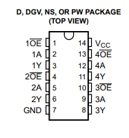
The SN74ALVC125 features independent line drivers with 3-state outputs. Each output is disabled when the associated output-enable (OE) input is high
To ensure the high-impedance state during power up or power down, OE should be tied to VCC through a pullup resistor; the minimum value of the resistor is determined by the current-sinking capability of the driver

热门型号
热门资讯
20万现货SKU
品类不断扩充
科技智能大仓储
4小时快速交货
仅从原厂和代理商进货
每一颗料均可原厂追溯
明码标价节省时间成本
一站式采购正品元器件


 工商网监
工商网监